
The MiniPA Linear amplifier for HF – in practice
QRP for HF is now popular – rigs such as the Yaesu FT818 or low power SDR transceivers are readily available. These are suitable for low power data modes or CW but struggle on SSB – many operators are looking for a step up with a linear amplifier. A full featured 100W amplifier will set you back anything up to US$1000.
But there are cheap kits sold on eBay and from Chinese suppliers such as AliBaba. These claim an SSB power output of 70-100W over the HF bands using cheap MOSFET switching transistors such as the IRF 530. For $US35 or so for the kit this seems excellent value.
But how good are they in practice?
The MiniPA is a design originally by ??. It uses a broadband balanced push-pull configuration with bias, PTT and changeover relay circuits. The 70W version uses two IRF530 MOSFETs designed for power switching applications. They are not optimized for RF with a quite a significant input capacitance which has to be “swamped” with resistance for broadband use.
But they are cheap at $1-2 ea and a useful amplifier can be made with these. There is a 100W version which uses a purpose designed dual RF transistor MRF9120 – I built this also for comparison.
I ordered one of these kits and it arrived several weeks later. There was no documentation, but there are many articles available on the internet. For the money it is good value with a well designed PCB populated with some surface mount parts and the components required to build the amp. It does not include a heatsink – this is definitely necessary for this design. Suitable heatsinks can be obtained separately. Ideally forced air cooling should be used for data modes or high duty cycle.
Building the kit
(1) Separate the transformer ends from the PCB by cutting the bridges to the PCB itself and filing down any rough spots. (Photos)
(2) Assemble T1 and T2 from their components – silver tube, ferrite core and two ends obtained from step (1). Solder the tubing to the PCB ends with a high power hot soldering iron. This allows this job to be done quickly with less damage to the components.
The silver tubing acts as a single half turn winding for the low impedance side of the transformer. Wind the other windings (3T for T1 and 5T for T2) using the plastic covered wire supplied. Leave the soldering to the board for later.
(3) Mount the various components except for the power transistors on the board referring to the PC overlay and circuit at XX Note that the relay pins must be bent laterally – there are no through hole components on the board. The choke L? used heavy enamelled copper wire – I changed this for heavy insulated hookup wire. Bear in mind this choke will have significant current through it – in theory up to 15A. The drain to gate feedback networks consisting of R?,? and C?,? are shown on the net circuit diagrams as 150R and 100n. The board has the 100n cap mounted and the 1W resistors supplied were 10R. There did not appear to be resistor in the kit across the input transformer secondary – various authors mention this to flatten the gain, swamp the input capacitance and improve input SWR
(4) You may have to drill the heatsink with mounting holes for the board and power transistors. I used M3 hardware and tapped the drill holes to accept this. I used an old heatsink from an audio power amplifier. Mount the power transistors using insulating hardware for the IRF530 and heatsink compound to improve thermal conduction and solder them to the board. Mount the RF transformers, ensuring that the transistor side connections are correctly aligned with the gap in the PC pads.

MRF9120 Version
The MRF9120 is a purpose designed RF Dual FET. This appears to work somewhat better than the switching FETs as one would expect. The case is connected to source and is common to the 2 transistors. It can be bolted to the heatsink direct without insulation. Gain was flatter over HF being about 13dB with the resistor across the input transformer of 27 ohms as supplied. I noted a resonance and possible instability at about 70 MHz. The device supplied had clearly been recovered from surplus equipment but appeared to function OK. There is a discussion on HF oscillation with these transistors on Google Groups at https://groups.google.com/g/hermes-lite/c/VhcNBjpEKMY
In short the MRF9120 was originally designed as an amplifier at 900 MHz. They have been discontinued production wise which is why many are recovered from surplus equipment and apparently “new” ones may be suspect. HF oscillation is an issue due to their gain at UHF. Several approaches have been suggested to cure this.
(1) capacitor across the feedback resistor to reduce gain at VHF
(2) Cut traces to the pads for the MRF530
(3) I tried a capacitor across the input transformer to provide a broad resonance at the upper HF range
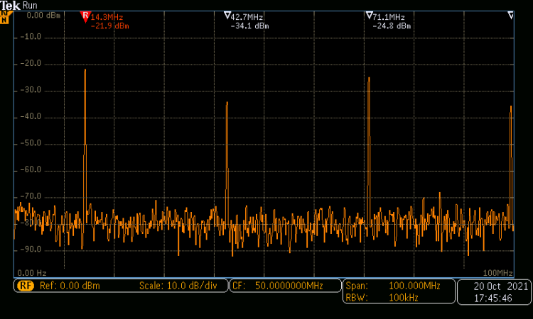
Spectrum analyser output of MRF9120 amplifier driven with +20dBm at 14.3MHz
Output is approx +30dBm – ie 10 dB gain. The second harmonic is well attenuated. The Third Harmonic is down only 13 dB and there is a strong 5th harmonic down barely 3dB, implying there is probably instability here
Testing
It is wise to use current limited supplies as it is easy to destroy the power transistors.
Connect a suitable 50 Ohm load to the output before powering up. It will need to be able to dissipate up to 100W or so. You will also need some sort of power metering. If you intend to perform harmonic and IMD tests you need suitable equipment such as a spectrum analyser
Set the the current limit low (say 200mA initially) and connect a 12-13.8V supply. Check polarity before powering up – there is no reverse protection diode!. Without the PTT enabled current should be zero. Check that the bias pot VR1 is at minimum.
Connect PTT by shorting the two pins. The relay should trigger and the board should be drawing 20mA or so. Adjust the bias pot VR1 for an idle current of 120mA. I did see some articles suggesting up to 1A idle current. This would improve linearity but heat dissipation is significant. I found that idle current increased steadily in a “thermal runaway” manner as the transistors heated up and it was difficult to get a steady current at this level.
Ideally the power supply should have current limiting – a common mode of transistor destruction seems to be overcurrent and overheating.
Power output
The quoted output of 70W appears difficult to achieve in practice with acceptable heat dissipation, harmonic and IMD performance
With a maximum drive of 5W power output of ?W was achieved
Gain
Gain varies over the HF bands dropping off to 6dB or so at 50 MHz
Harmonics
Second order harmonics (2nd, 4th etc) are well attenuated due to the balanced design but the third order harmonic was barely 5dB down on the fundamental with a quiescent current of 120mA. The balanced design eases the specs for low pass filters but these are definitely necessary
IMD
This is the usual method of linear amplifier assessment
It requires a two tone source – in this case I have driven the FT 818 with two audio tones and 500 Hz and 2500Hz
at a drive level of 1W and 20W output 3rd order products are dB down
Increasing this to 2W =>
and 5W =>
Newer devices
In the last 3 years or so new LDMOS devices have become available.
These offer much higher power gain up to 28dB – a single stage amplifier could deliver 1KW or more when driven by an FT 818 with 5 W output!
They are rugged and relatively cheap for these power levels
Of course in Australia we are limited in power output so I set about designing a 100W board with the MRF101 devices which are available from local suppliers at $35 each. For a legal limit amplifier using easily available devices, there is an excellent article by Razvan Fatu at https://qrpblog.com/2019/10/a-600w-broadband-hf-amplifier-using-affordable-ldmos-devices/
Cooling and monitoring is important with high power amplifiers. I also set about designing a board to monitor supply current, output power, SWR and device temperature with circuits to shut the amplifier down if these are out of range.
